News
RFID ISO 14443A Tag selection
Learn about RFID tag circuit design and NFC chip selection, covering protocols (ISO14443A/B, ISO15693), LPCD low-power detection, and financial certifications (PBOC/EMV). Explore RFID system architecture: power circuits, SPI/I2C interfaces, and antenna tuning (EMC filtering, matching circuits, PCB layout). Optimize RFID tag circuits for performance with guidelines on antenna size, winding, and component precision. Essential for RFID engineers and hardware developers.

NFC (Near Field Communication) chip selection:
Key Considerations:
protocols supported by the chip, whether it supports low-power card detection, whether it can pass financial certification, chip price
Protocols supported by the chip:
ISO14443A/B, ISO15693, ISO18092 and ISO21481, etc.
ISO14443A card: Mifare series, Ultralight series, Plus series, CPU card series, etc.
ISO14443B cards: ID cards, SR176, SRI512, etc.
ISO15693: NXP's ICODE series, TI's Tag_it HF-I, ST LRI, and so on.
ISO18092: including read mode, card mode, point-to-point communication mode.
ISO21481: Compatible with ISO15693 protocol based on ISO18092.
LPCD Function: The chip detects the card with low power consumption. When there is no card close to the chip, the chip is in a low-power state, only 10uA current, can complete the card detection, when the card is close to the chip detects the card, wake up the microcontroller to read the card.
Financial authentication: PBOC2.0/3.0 standard, EMV standard.
Circuit architecture:
The external circuit of NFC chip usually consists of the following parts: power supply circuit, communication interface circuit, antenna circuit, oscillation circuit;
Power supply circuit: It mainly includes analog power supply AVDD, digital power supply DVDD, transmitter power supply TVDD, pin power supply PVDD, and test pin power supply PVDD2 ;
a. If you need to increase the transmitter power, you can increase the voltage of TVDD, for example, the transmitter power formed by the 5V supply TVDD will be stronger than the 3V one;
b. The power supply current of the chip is usually in the range of tens to hundreds of mA, and the main energy consumption is in the transmitter circuit. For example, the antenna of FM175xx has a transmitting current of 100mA, while RC663 has a current of 250mA. Therefore, it is necessary to pay attention to sufficient margin when choosing the power supply chip and inductors;
c. The 13.56MHz sine wave signal of the antenna of the card reader chip will interfere with the power supply, in order to reduce the conduction interference, you can add a π-type filter on the power supply side, but in order to reduce the redundancy of the circuit design, it is not added under normal circumstances.
Communication interface:
usually support SPI/I2C/UART, generally through the external pin configuration options, in order to facilitate the upgrade, compatible design;
Antenna Design:
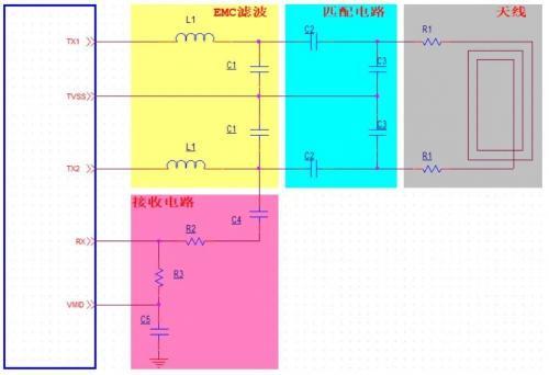
antenna circuit is mainly composed of 4 parts: EMC filtering, matching circuit, antenna, receiving circuit. Take FM17550 as an example, as follows:
Filter circuit:
by L1, C1 composed of low-pass filter used to filter out 13.56MHz derived harmonics, the filter cutoff frequency should be designed above 14MHz. L1 inductors can not be placed close to each other, so as not to interfere with each other (mutual inductance effect). Filter circuit element matching formula: f=1/(2π√LC)
Matching circuit:
is used to adjust the transmitter load and resonant frequency. The power of the RF circuit is affected by the internal resistance and external impedance of the chip, when the internal resistance and external impedance of the chip are the same, the transmitting power efficiency is the highest.C2 is the load capacitance, the larger the antenna inductance, the smaller the value of C2.C3 is the resonance capacitance, the value of the resonant capacitance is directly related to the antenna inductance, which makes the resonance frequency at 13.56MHz.
Receiver circuit:
C4 filters the DC signal, R2 and R3 form a voltage divider circuit, so that the amplitude of the sine wave signal at the RX receiver is between 1.5-3V.
Antenna:
consists of R1 resistor (usually 1ohm or 0ohm) and printed PCB.
The larger the antenna is, the farther the reading distance will be. When the antenna area reaches 5cm x 5cm, the reading distance will not be significantly improved if the antenna is enlarged.
Antenna line width is recommended to choose 0.5mm - 1mm, antenna larger than 5cm x 5cm can not be more than 3 turns, smaller than 3cm x 3cm can not be less than 4 turns.
In order to minimize the EMC radiation interference, it is necessary to draw the corner of the PCB alignment into a round arc.
Inside the antenna area and the edge of the antenna, signal, power, ground line is prohibited to be drawn into a circle or semicircle, and the antenna coil should not have large metal objects and metal coating, to avoid causing the magnetic field eddy current effect resulting in serious loss of capacity.
Antenna PCB winding way is relative, not isotropic.
The precision of antenna circuit design components should be controlled within 2%, otherwise it is easy to lead to the antenna resonance frequency deviation, resulting in a serious decline in the performance of the card reader, the consistency of the product is difficult to guarantee.
Antenna size and reading distance relationship

Categories
Latest News
Contact Us
SEIKO RFID TECHNOLOGY LTD.
Add: Rm.7127, No.350, Changle Rd., Huli District, Xiamen 361006, China.
Tel: 0595-22586002
Email: sales@seikorfid.com
Phone: +86-18559272337 (WhatsApp)